Our client investigates how microscopic changes in a material’s structure influence its performance in electronic applications. After completing his undergraduate and master’s studies at Izmir Institute of Technology, he earned a Ph.D. in mechanical engineering at the University of California, Merced. His doctoral research used scanning probe microscopy to examine defects and strain in emerging electronic materials. He subsequently joined the University of North Dakota as a postdoctoral research fellow, working on semiconductor synthesis and advanced materials characterization.
Our firm presented a petition connecting this research background to his plans for developing more reliable thin films and two-dimensional materials. Supporting evidence included five peer-reviewed research articles, academic collaborations, student mentoring, and industry experience as a materials and surface science intern at ASML. We explained how his proposed combination of controlled material growth and atomic-scale analysis could inform the development of energy-efficient transistors, sensors, and materials for quantum technologies.
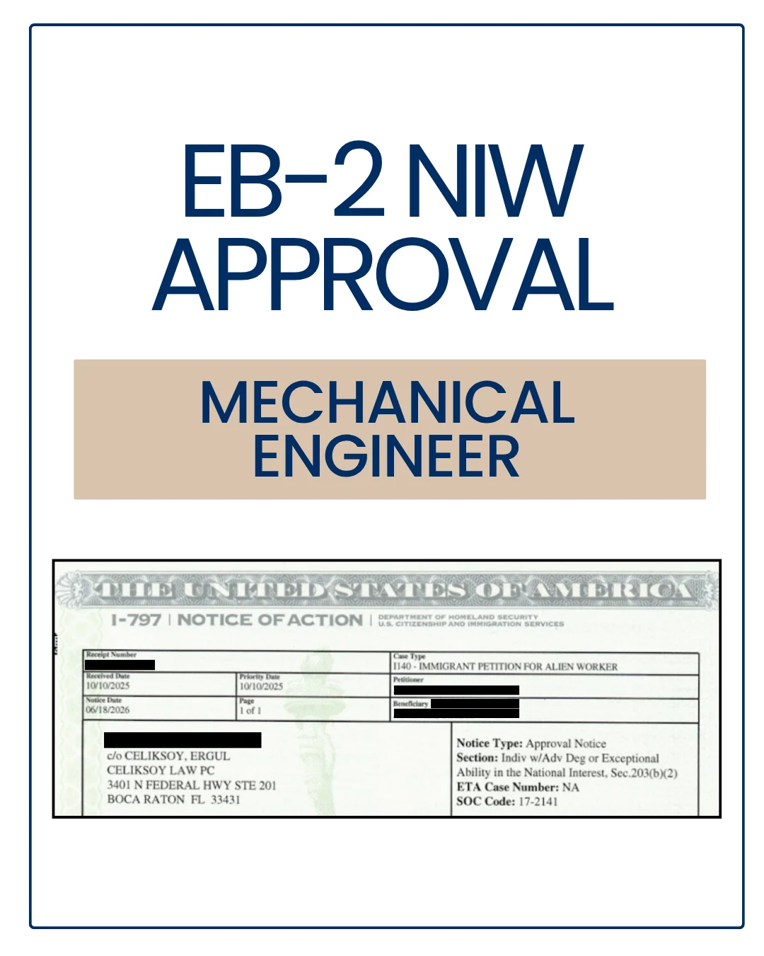
His experience at ASML gave the case a practical connection to semiconductor manufacturing, complementing his university research into how materials behave at the atomic level. The petition drew on both settings to explain his ability to investigate fundamental material properties while understanding the reliability challenges faced by industry. USCIS approved his I-140 petition under the EB-2 National Interest Waiver category, advancing his plans to contribute to semiconductor research and innovation in the United States.