
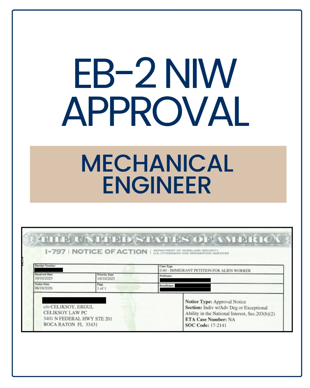
Celiksoy Law secured EB-2 National Interest Waiver approval for a mechanical engineer researching semiconductor materials, thin films, and two-dimensional crystals. His petition connected atomic-scale investigations of defects and strain with a proposed U.S. research program aimed at improving how emerging electronic materials are grown, measured, and evaluated for device applications.
A distinctive feature of this case was the connection between university research and industry experience. Alongside his work on nanoscale material properties, our client had investigated surfaces and contamination during an internship involving semiconductor manufacturing equipment. The petition used both settings to explain his preparation for research addressing material reliability and fabrication challenges.
Mechanical engineering applied to electronic materials
Our client’s academic background included undergraduate, master’s, and doctoral study in mechanical engineering. His master’s work involved optimizing laminated composites for structural stability. His doctoral research moved to a much smaller scale, using scanning probe microscopy to investigate defects and strain in emerging electronic materials.
That progression linked mechanical behavior with electrical properties. In the research presented in his petition, a material’s performance depended on more than its chemical composition: local defects, surface structure, and mechanical deformation could affect how it conducted electricity or responded to contact and wear.
The record also described U.S. postdoctoral research involving thin-film synthesis and characterization. His experience combined material growth techniques with microscopy and surface analysis, supporting the proposed transition from observing material behavior to investigating ways of controlling it.
The proposed U.S. research program
The proposed endeavor brought together three connected areas of work.
Controlled growth of thin films and two-dimensional materials. The client proposed refining molecular beam epitaxy and chemical vapor deposition methods to investigate how growth conditions influence defects, strain, and material quality. The goal was to develop more reproducible approaches to materials relevant to emerging electronic technologies.
Atomic-scale analysis of structure and performance. He planned to combine scanning probe microscopy with electron microscopy and spectroscopy to study how local structural features affect electrical and mechanical behavior. These methods would help identify mechanisms relevant to defect repair, surface treatment, and integration of materials into devices.
Research toward electronic applications. The program sought to connect these findings with possible pathways for low-power transistors, sensors, and materials relevant to quantum technologies. Device integration and scalable manufacturing were objectives for further research, supported by the proposed methods and collaborations.
The petition explained the potential broader contribution through these specific technical questions. More reliable growth and better understanding of material behavior could inform work across research laboratories and semiconductor development teams. His research plan therefore connected an identifiable scientific problem with potential uses beyond a single research position.
Research findings supported the proposed direction
The publication record helped show how his experience related to the work he proposed to pursue.
Defect repair and material reliability. A collaborative study of monolayer molybdenum disulfide examined how chemical treatment affected mechanical reliability and the uniformity of electrical behavior. The client contributed conductive atomic force microscopy work that helped characterize local electronic properties. This linked his expertise in nanoscale measurement to a practical question: whether treating defects could improve a material’s behavior under experimental testing.
Strain and electronic properties. A first-author study of thin molybdenum carbide crystals combined local electrical measurements with calculations to investigate how tensile strain influenced conductivity and work function. Work function describes the energy needed to remove an electron from a material’s surface. A separate computational study examined how strain and defects altered electronic structure and hydrogen adsorption on molybdenum carbide surfaces. These studies connected mechanical changes with electronic and surface behavior, while serving different experimental and theoretical purposes.
Thin-crystal growth. A coauthored synthesis study investigated a graphene-driven route for growing ultrathin molybdenum carbide. The experimental approach used graphene as the carbon source and examined a route toward graphene-free crystals. It supported the materials-growth aspect of the endeavor without establishing commercial production readiness.
Surface measurement and methods. His work also included first-author nanoscale friction research on alloy sulfide films and a first-author perspective on scanning probe microscopy of MXenes, a family of two-dimensional materials. The friction study supported his surface-measurement experience. The perspective assessed existing methods and future opportunities, complementing his original experimental publications.
Industry experience added a manufacturing connection
During a materials and surface science internship, the client used microscopy, spectroscopy, and surface measurement techniques to investigate semiconductor equipment components and test systems. The petition described work involving particle and molecular contamination and interactions at material surfaces.
His supervisor’s reference letter explained how these investigations provided input to engineering teams addressing contamination control. This experience helped connect the academic research to practical equipment questions. The petition presented it as an internship with defined technical responsibilities and professional feedback.
His teaching and mentoring activities added another dimension. The record described engineering instruction, guidance on experimental methods and data analysis, teaching evaluations, and teaching recognition. These materials supported experience communicating technical concepts and helping students develop research skills.
The evidence and its role in the petition
| Evidence described in the petition | Role in the presentation |
|---|---|
| Mechanical engineering degrees and doctoral research | Established advanced training and a research background connecting mechanics with electronic materials. |
| Thin-film and postdoctoral research experience | Supported familiarity with synthesis, microscopy, and materials characterization relevant to the endeavor. |
| Experimental and computational publications | Connected completed research with defect repair, strain, surface properties, and material growth. |
| Microscopy perspective article | Demonstrated analysis of existing methods and research opportunities; distinguished from original experimental work. |
| Citations to published work | Documented use of his research in the literature, with examples described in the petition. |
| Industry internship records and supervisor letter | Explained his responsibilities and contribution to surface and contamination investigations. |
| Conference records | Supported scientific dissemination, distinguishing presentation records from attendance certificates. |
| Research fellowships and recognition | Documented research support, teaching recognition, and separate presentation or scientific imaging distinctions. |
| Teaching evaluations and mentoring confirmation | Supported his role in engineering education and research training. |
| Independent expert and reference letters | Provided technical context, with independent opinions separated from accounts by advisers, collaborators, and supervisors. |
| Proposed endeavor statement | Defined the research objectives and their relationship to his experience and potential wider contribution. |
Connecting the evidence to the NIW argument
We presented the case around the relationship between the client’s technical methods, documented contributions, and future research objectives. The publication evidence explained the scientific foundation. His industry experience showed familiarity with practical surface-related problems. Expert and reference letters helped explain his individual role within collaborative work.
The petition argued that the proposed research could contribute to broader semiconductor development through knowledge about material growth, defects, and reliability. It also explained why his combination of academic and industry experience positioned him to advance that work. We presented the significance of the endeavor through its proposed contribution, supported by the applicant’s record.
USCIS approved the EB-2 NIW petition. The approval notice confirms the outcome but does not describe the agency’s assessment of individual publications or evidence items.
At Celiksoy Immigration Lawyers, we assess researchers’ qualifications, proposed U.S. endeavors, and supporting evidence together. To discuss an EB-2 NIW petition, contact us at us@celiksoylaw.com. Each case is assessed on its own facts and evidence.